Product Summary
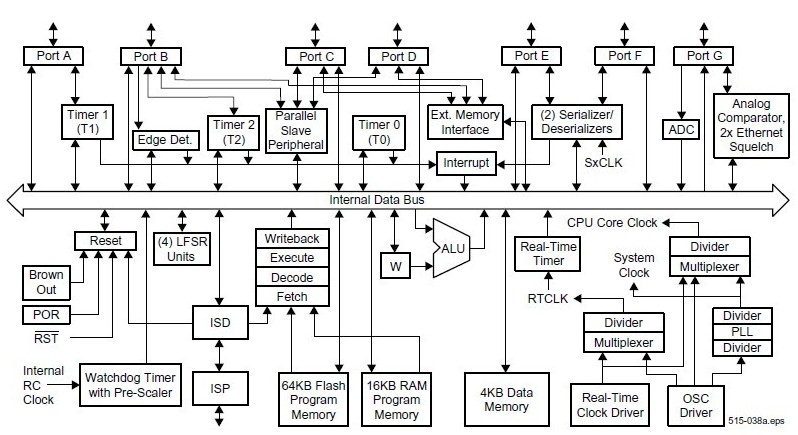
The IP2022PQ80-120 is a kind of Internet Processor which combines support for communication physical layer, Internet protocol stack, device-specific application, and devicespecific peripheral software modules in a single chip, and is reconfigurable over the Internet. The IP2022PQ80-120 can be programmed, and reprogrammed, using pre-built software modules and configuration tools to create true single-chip solutions for a wide range of device-to-device and device-to-human communication applications.
Parametrics
IP2022PQ80-120 absolute maximum ratings:(1)Ambient temperature under bias: -40 to 85℃; (2)Storage temperature: -65 to 150℃; (3)Voltage on DVdd with respect to Vss: -0.5 to 3.5 V; (4)Voltage on XVdd with respect to Vss: -0.5 to 3.5 V; (5)Voltage on AVdd with respect to Vss: -0.5 to 3.5 V; (6)Voltage on GVdd with respect to Vss: -0.5 to 3.5 V; (7)Voltage on IOVdd with respect to Vss: -0.5 to 4.5 V; (8)Voltage on Port A through Port F, OSC1, RST, RTCLK1, TSCK, TSI, and TSS inputs with respect to Vss: -0.5 to 5.7 V; (9)Voltage on Port G inputs with respect to Vss: -0.5 to 3.5 V; (10)Total power dissipation: 1 W; (11)Maximum current out of all DVss pins: 400 mA; (12)Maximum current into all DVdd pins: 400 mA; (13)Maximum allowable sink current per I/O pin: 160 mA; (14)Maximum allowable source current per I/O pin (excluding port G): 160 mA; (15)Maximum allowable source current per G pin: 20 mA; (16)Maximum allowable sink current per group of I/O pins between IOVss pins: 160 mA; (17)Maximum allowable source current per group of I/O pins between IOVdd pins (excluding port G): 160 mA; (18)Latchup: 200 mA; (19)θJA, 80-pin PQFP Package: 48℃/W; (20)θJA, 80-pin μBGA Package: 37℃/W; (21)Flash block erase cycle lifetime (if using 20ms block erases - Section 7.1.5): 20K Cycles min; (22)Flash bulk erase cycle lifetime: 20K Cycles min; (23)ESD Human Body Model - all pins: 1500 V min; (24)ESD Machine Model - all pins: 200 V min.
Features
IP2022PQ80-120 features: (1)Designed to support single-chip networked solutions: Fast processor core; 64kB Flash program memory; 20kB SRAM data/program memory; Two SerDes communication blocks supporting common PHYs (Ethernet, USB, UARTs, etc.) and bridging applications; (2)Advanced 120 MIPS RISC processor: High speed packet processing; Instruction set optimized for communication functions; Supports software implementation of traditional hardware functions; (3)In-system reprogrammable for highest flexibility: Run time self-programmable; Vpp = Vcc supply voltage.
Diagrams

 |
 IP20 |
 Sola/Hevi-Duty |
 Fuseholders, Clips, & Hardware PLASTIC TOUCH PROOF COVER KIT |
 Data Sheet |

|
|
||||||||||||
 |
 IP200 |
 Other |
 |
 Data Sheet |
 Negotiable |
|
||||||||||||
 |
 IP2001 |
 International Rectifier |
 Switching Converters, Regulators & Controllers |
 Data Sheet |

|
|
||||||||||||
 |
 IP2001PBF |
 |
 IC REG BUCK SYNC ADJ 20A 144BGA |
 Data Sheet |

|
|
||||||||||||
 |
 IP2001TR |
 International Rectifier |
 Switching Converters, Regulators & Controllers |
 Data Sheet |

|
|
||||||||||||
 |
 IP2001TRPBF |
 |
 IC REG BUCK SYNC ADJ 20A 144BGA |
 Data Sheet |

|
|
||||||||||||
 (China (Mainland))


